Icom
Interface Level Translator
OVERVIEW:
Some of the
vintage Icom radio use a bus that is based on 9V instead of 5V. The interface
uses 5V so for use on the 9V systems, the signals must be converted to 9V
levels. In addition to the voltage translation, the level Translator needs to
be bidirectional for most of the interface logic signals. This bidirectional
level shifter is based on a decades old circuit that was used to level shift
I2C bus voltages from one bus with a 5V bus to another bus of a different
voltage. It appears in Phillips Application note AN97055. In case any
troubleshooting is needed, the applicable pages of the app note are at the end
of this webpage.
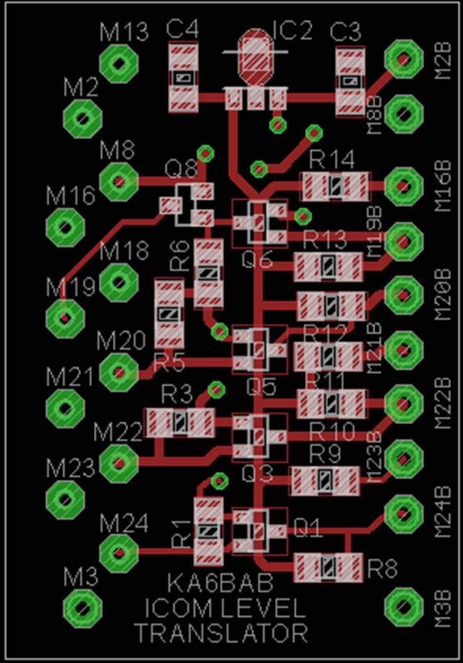
The schematic is shown in Figure 1. There is a 5V and 9V
side, with each having its own dedicated regulator. Conceptually, this board is
placed between the radio and the interface board. The +12V, GND, and PTT
signals pass thru the translator board and go directly to the main interface
board. The +12V and GND signals are also used by this board to produce the 5V
and 9V through the regulators. The RC and ANALOG signal are not passed through
because those signals are never user on any of the radios with a 9V processor.
All of the remaining signals are digital. One of the signals on M19 or the “DV”
is unidirectional, and required an open collector output.
The “M” numbers on the left side of the schematic, like
“M24” connect directly to the pin of the same name on the interface board. The
corresponding “M24B” connects to the 24-pin accessory connector where “M24”
would usually be on a radio that did not need level converting. The connection
between the level translator can be made with wires, or the wire holes are
spaced so that one board can rest on the other, as shown in Figure 3. There
will be some SMD parts in between the boards, so it is necessary to determine
if any insulation or separation between the boards is necessary.
The parts list is contained in Table 1. There are no exotic
or tiny parts. Installation should be simple.

Figure
1. Schematic Diagram for the Translator Board
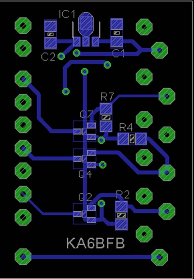
Figure
2 Top (left) and bottom layer artwork for the translator board
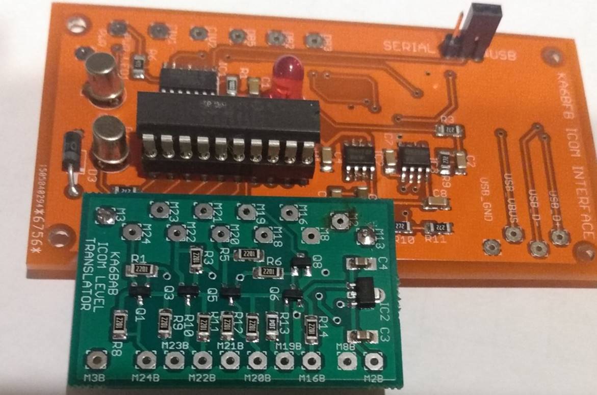
Figure
3. Finished translator board mounted directly on interface board
|
Part |
Value |
Package |
Comment |
Digikey P/N |
|
C1-C4 |
CAP, .1uF, 50V |
1206 |
|
399-1177-1-ND |
|
IC1 |
L78L05ACUTR, 5V REG |
SOT89-3 |
|
497-1183-1-ND |
|
IC2 |
L78L09ACUTR, 9V REG |
SOT89-3 |
|
497-1192-1-ND |
|
Q1-Q7 |
2N7002, MOSFET N CH |
SOT23 |
|
2N7002LT1GOSCT-ND |
|
Q8 |
MMBT3904, NPN 40V |
SOT23 |
|
MMBT3904-FDICT-ND |
|
R1-R5,R7-R12,R14 |
2.2K, 1% |
1206 |
|
CR1206-FX-2201ELFCT-ND |
|
R6 |
22k, 5% |
1206 |
|
RMCF1206JT22K0 |
|
R13 |
100k, 5% |
1206 |
|
P100KECT-ND |
|
PCB |
|
|
Available from KA6BFB for $25 plus shipping |
N/A |
Table
1. Parts List
TESTING:
Testing is straightforward and simple. Temporarily tack
solder two wires from a power supply set to +12V output to M2 and M8. Verify
the proper output of the 5V and 9V regulators. Six of the translator circuits
are electrically identical. We will test them first. The inputs on both sides
are pulled high and stay that way until pulled low. A low on one side is
transferred to the other side Starting from the left side of the schematic, use
a clip lead to ground the left side of each of the
identical translators, and confirm the corresponding output on the right side
goes low. Remove the ground and verify the corresponding output on the right
side goes high. Now reverse the situation. Ground each of the inputs on the
right side and verify that its corresponding output on the left side goes low.
Verify the left side output goes high when the ground is released on the right
side.
To test the Q6/Q8 path, solder one side of a 10k resistor
(through hole) temporarily to M19, and the other end to +12V. Confirm the
voltage on M19 is low. Ground M19B with a clip lead and verify M19 goes high.
Remove the clip lead and verify M19 returns to a low state. Remove the temporary 10k resistor and the
wires on M2 and M8 and wire the translator to the interface board and the
24-pin accessory connector.
The following is an excerpt from Philips Application Note
AN97055. This might be useful if troubleshooting is needed
Devices
with different logic levels connected via the bi-directional level shifter.
The bi-directional level shifter is used to interconnect
two sections of an I2C-bus system, each section with a different supply voltage
and different logic levels. In the bus system of Figure 4 the left section has
pull-up resistors and devices connected to a 3.3 Volt supply voltage, the right
section has pull-up resistors and devices connected to a 5 Volt supply voltage.
The devices of each section have I/O’s with supply
voltage related logic input levels and an open drain output configuration.
The
level shifter for each bus line is identical and consists of one discrete
N-channel enhancement MOS-FET, T1 for the serial data line SDA and T2 for the
serial clock line SCL. The gates (g) has to be connected to the lowest supply
voltage VDD1 , the sources (s) to the bus lines of the
“Lower voltage” section, and the drains (d) to the bus lines of the “Higher
voltage” section. Many MOS-FET’s have the substrate internally already
connected
with its source, otherwise it should be done externally. The diode between the
drain (d) and substrate is inside the MOS-FET present as n-p junction of drain
and substrate.
Description of the
level shift operation.
For
the level shift operation three states has to be considered:
·
State
1. No device is pulling down the bus line and the bus line of the “Lower
voltage” section is pulled up by its pull-up resistors Rp to 3.3 V. The gate
and the source of the MOS-FET are both at 3.3 V, so its VGS is below the
threshold voltage and the MOS-FET is not conducting. This allows that the bus
line at the “Higher voltage” section is pulled up by its pull-up resistor Rp to
5V. So, the bus lines of both sections are HIGH, but at a different voltage
level.
·
State
2. A 3.3 V device pulls down the bus line to a LOW level. The source of the
MOS-FET becomes also LOW, while the gate stays at 3.3 V. The VGS rises above
the threshold and the MOS-FET becomes conducting. Now the bus line of the
“Higher voltage” section is also pulled down to a LOW level by the 3.3 V device
via the conducting MOS-FET. So the bus lines of both
sections become LOW at the same voltage level.
·
State
3. A 5 V device pulls down the bus line to a LOW level. Via the drain-substrate
diode of the MOSFET the “Lower voltage” section is in first instance pulled
down until VGS passes the threshold and the MOS-FET becomes conducting. Now the
bus line of the “Lower voltage” section is further pulled down to a LOW level
by the 5 V device via the conducting MOS-FET. So, the bus lines of both
sections become LOW at the same voltage level.
.
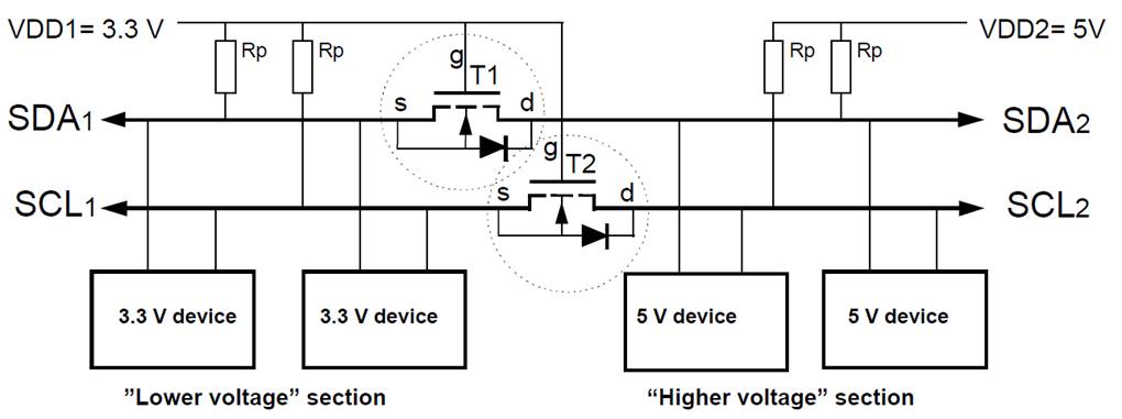
Figure
4. Bi-directional level shifter circuit connects two different voltage sections
of an I2C-bus system.
The
three states show that the logic levels are transferred in both directions of
the bus system, independent of the driving section. State 2 and state 3 perform
the “wired AND” function between the bus lines of both sections as required by
the I2C-bus specification. Other supply voltages than 3.3V for VDD1 and 5V for
VDD2 can be applied, e.g. 2V for VDD1 and 10V for VDD2
is feasible. In normal operation VDD2 must be equal to or higher than VDD1.